
chemical etching process for sem manufacturer Grasping strong production capability, advanced research strength and excellent service, Shanghai chemical etching process for sem supplier create the value and bring values to all of customers.
 WhatsApp)
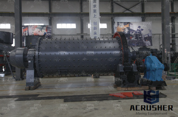
The Preparation of Silicon Nanowires Using MetalAssisted ... Silicon Nanowires Using MetalAssisted Chemical ... Chemical Etching, Silicon Nanowires, SEM.
... does not possess the ability to etch BST thin films annealed at high temperature, ... microscope (SEM) ... during the wet chemical etching process due to ...
Plasma Etching Outline ... Ideal Etching Process substrate film to be etched mask Before etch substrate ... Chemical Etching Ion Beam Methods Dry Etching
... we have developed a novel method for Pt etching using a chemical dry etching ... under various etching conditions. Chemical analysis of ... SEM studies of the Pt ...
This paper describes the optimized process of wetchemical etching of a ZnO ... the ZnO films to serve as the etching mask. The SEM photography of the etched sample ...
Metalassisted chemical etching in HF ... etching process. ... Topview SEM images of Ptcoated Si~100! after etching in
... dissolution of agarose stamp into hot water demonstrates an environmentally friendly method by the moldassisted chemical etching process ... SEM images of ...
Alkali Anisotropic Chemical Etching of P ... SEM and FTIR spectroscopy. The ... The process of wet alkali anisotropic chemical etching process was monitored as the ...
Chemical Etching of Natural Fluorapatite Crystals in Acid Solutions Studied ... Different aspects of the chemical etching process ... chemical etching, fluorapatite, SEM
WetChemical Etching and Cleaning of Silicon ... following is a typical RCA process; ... with all wetchemical etching solutions, ...
To analyze the chemical etching process of InAs/GaSb ... SEM image of a cleaved mesa of the diode etched with the H 3PO 4/H 2O 2/H 2O solution at RT is shown in ...
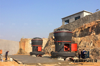
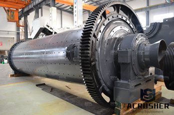
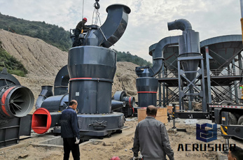
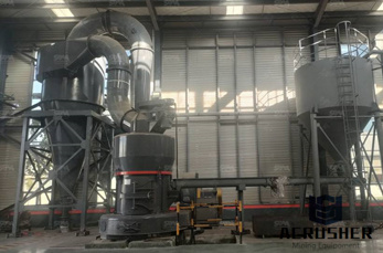
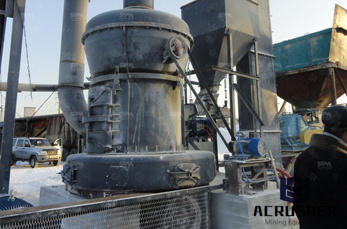
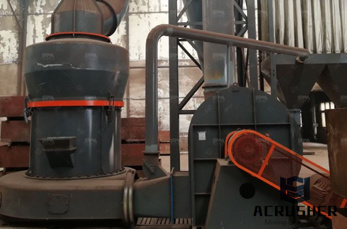
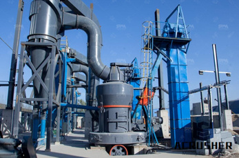
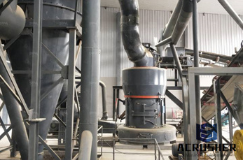
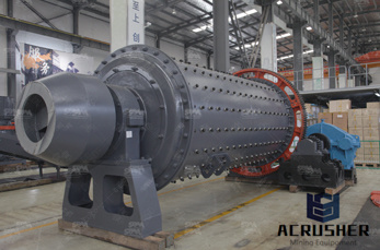
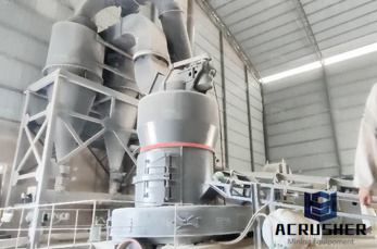
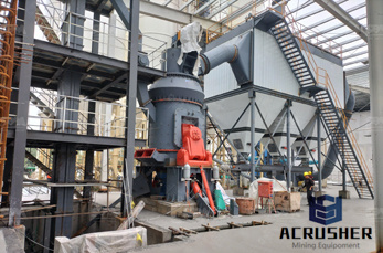
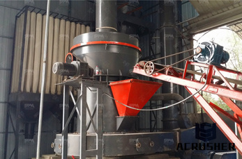
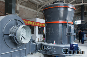
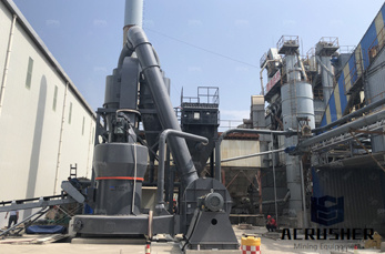
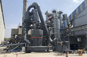
Home > Mining News > chemical etching process for sem. Information. Crushing Equipment; Grinding Equipment; Feeding Conveying; Screening Washing; Mobile .
chemical etching process. The chemical etchant used to ... Crosssectional SEM image of LEO GaN epilayer before etching process. (b–f) ...
How to Acid Etch Steel. ... sulfate from coating the steel with a deposit of copper that will stop the etching process. ... The etching chemical, ...
Electron induced chemical etching/deposition ... be observed by the SEM. The etching and deposition ... an etching process may be analyzed to ...
present an original experiment by SEM on how it responds to the etching with ... SEM Analysis of the Effectiveness of the Acid Etching ... in the chemical attack ...
Effects of the Nitric Acid Concentrations on the Etching Process, ... of porous zinc oxide by wet chemical etching. ... etching time, as discussed in SEM ...
Etching Methodologies in 111 Oriented Silicon ... Abstract— New methodologies in anisotropic wetchemical etching of 111 oriented silicon, allowing useful process ...
This sequence of patterning and etching is repeated multiple times during the chip making process. Etch processes ... physical and chemical etching such ...
Wet and Dry Etching ... chemical etching, ... A wet etching process involves multiple chemical reactions that consume the original reactants
Wet Chemical Etching Process of BST Thin Films for Pyroelectric Infrared Detectors. ... Wet Chemical Etching Process of BST Thin Films for Pyroelectric Infrared ...
A 3D Simulator for Silicon Anisotropic Wet Chemical Etching Process ... anisotropic etching process simulation ... chemical etching of crystalline ...
... assisted chemical etching process in ... chemical etching process on lithographically ... lithographically defined areas formation kinetics ...
Electronassisted chemical etching of ... alterations that occur during electronassisted chemical etching of ... chemical etching process, ...
WhatsApp)